- 您现在的位置:买卖IC网 > Sheet目录368 > W631GG6KB-15 (Winbond Electronics)IC DDR3 SDRAM 1GBIT 96WBGA
�� �
�
�W631GG6KB�
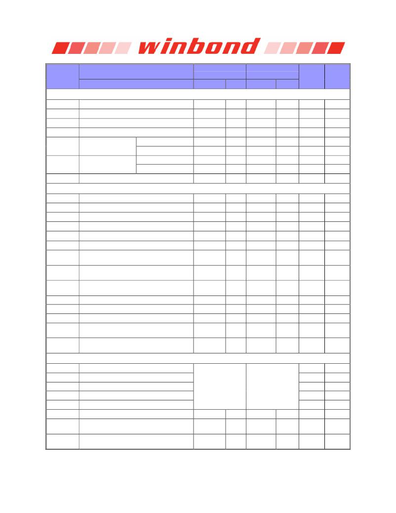
�AC� Timing� and� Operating� Condition� for� -12/12I/12A/12K/-15/15I/15A/15K� speed� grades,� continued�
�SYMBOL�
�SPEED� GRADE�
�PARAMETER�
�DDR3-1600�
�(-12/12I/12A/12K)�
�MIN.�
�MAX.�
�DDR3-1333�
�(-15/15I/15A/15K)�
�MIN.�
�MAX.�
�UNITS�
�NOTES�
�Data� Timing�
�t� DQSQ�
�t� QH�
�t� LZ(DQ)�
�t� HZ(DQ)�
�t� DS(AC150)�
�t� DH(DC100)�
�t� DIPW�
�DQS,� DQS#� to� DQ� skew,� per� group,� per� access�
�DQ� output� hold� time� from� DQS,� DQS#�
�DQ� low� impedance� time� from� CK,� CK#�
�DQ� high� impedance� time� from� CK,� CK#�
�Base� specification�
�Data� setup� time� to�
�DQS,� DQS#�
�V� REF� @� 1� V/nS�
�Base� specification�
�Data� hold� time� from�
�DQS,� DQS#�
�V� REF� @� 1� V/nS�
�DQ� and� DM� input� pulse� width� for� each� input�
�?�
�0.38�
�-450�
�?�
�10�
�160�
�45�
�145�
�360�
�100�
�?�
�225�
�225�
�?�
�?�
�0.38�
�-500�
�?�
�30�
�180�
�65�
�165�
�400�
�125�
�?�
�250�
�250�
�?�
�pS�
�t� CK� (avg)�
�pS�
�pS�
�pS�
�pS�
�pS�
�23�
�18,� 23�
�17, 23, 24�
�17,� 23,� 24�
�11,� 40�
�11, 40, 42�
�11,� 40�
�11, 40, 42�
�10�
�Data� Strobe� Timing�
�t� RPRE�
�t� RPST�
�DQS,DQS#� differential� READ� Preamble�
�DQS,DQS#� differential� READ� Postamble�
�0.9�
�0.3�
�Note 21�
�Note 22�
�0.9�
�0.3�
�Note� 21�
�Note� 22�
�t� CK� (avg)� 18, 21, 23�
�t� CK� (avg)� 18, 22, 23�
�t� QSH�
�t� QSL�
�t� WPRE�
�t� WPST�
�t� DQSCK�
�t� LZ(DQS)�
�t� HZ(DQS)�
�t� DQSL�
�t� DQSH�
�t� DQSS�
�t� DSS�
�t� DSH�
�DQS,DQS#� differential� output� high� time�
�DQS,DQS#� differential� output� low� time�
�DQS,DQS#� differential� WRITE� Preamble�
�DQS,DQS#� differential� WRITE� Postamble�
�DQS,DQS#� rising� edge� output� access� time� from�
�rising� CK,� CK#�
�DQS� and� DQS#� low-impedance� time� from�
�CK,� CK#� (Referenced� from� RL� -� 1)�
�DQS� and� DQS#� high-impedance� time� from�
�CK,� CK#� (Referenced� from� RL� +� BL/2)�
�DQS,DQS#� differential� input� low� pulse� width�
�DQS,DQS#� differential� input� high� pulse� width�
�DQS,DQS#� rising� edge� to� CK,CK#� rising� edge�
�DQS,DQS#� falling� edge� setup� time� to� CK,CK#�
�rising� edge�
�DQS,DQS#� falling� edge� hold� time� from� CK,CK#�
�rising� edge�
�0.4�
�0.4�
�0.9�
�0.3�
�-225�
�-450�
�?�
�0.45�
�0.45�
�-0.27�
�0.18�
�0.18�
�?�
�?�
�?�
�?�
�225�
�225�
�225�
�0.55�
�0.55�
�0.27�
�?�
�?�
�0.4�
�0.4�
�0.9�
�0.3�
�-255�
�-500�
�?�
�0.45�
�0.45�
�-0.25�
�0.2�
�0.2�
�?�
�?�
�?�
�?�
�255�
�250�
�250�
�0.55�
�0.55�
�0.25�
�?�
�?�
�t� CK� (avg)�
�t� CK� (avg)�
�t� CK� (avg)�
�t� CK� (avg)�
�pS�
�pS�
�pS�
�t� CK� (avg)�
�t� CK� (avg)�
�t� CK� (avg)�
�t� CK� (avg)�
�t� CK� (avg)�
�18,� 23�
�18,� 23�
�46�
�46�
�17,� 23�
�17,� 23,� 24�
�17,� 23,� 24�
�12,� 14�
�13,� 14�
�16�
�15,� 16�
�15,� 16�
�Comman� d� and� Address� Timing�
�t� AA�
�t� RCD�
�Internal� read� command� to� first� data�
�ACT� to� internal� read� or� write� delay� time�
�nS�
�nS�
�8�
�8�
�t� RP�
�t� RC�
�t� RAS�
�PRE� command� period�
�ACT� to� ACT� or� REF� command� period�
�ACT� to� PRE� command� period�
�See� ―Speed� Bin‖� on�
�page� 135�
�See� ―Speed� Bin‖� on�
�page� 134�
�nS�
�nS�
�nS�
�8�
�8�
�8�
�t� DLLK�
�t� RTP�
�t� WTR�
�DLL� locking� time�
�Internal� READ� Command� to� PRECHARGE�
�Command� delay�
�Delay� from� start� of� internal� write� transaction� to�
�internal� read� command�
�512�
�max(4nCK,�
�7.5nS)�
�max(4nCK,�
�7.5nS)�
�?�
�?�
�?�
�512�
�max(4nCK,�
�7.5nS)�
�max(4nCK,�
�7.5nS)�
�?�
�?�
�?�
�nCK�
�8�
�8,� 26�
�Publication� Release� Date:� Dec.� 09,� 2013�
�Revision� A05�
�-� 143� -�
�发布紧急采购,3分钟左右您将得到回复。
相关PDF资料
W9412G6IH-5
IC DDR-400 SDRAM 128MB 66TSSOPII
W9412G6JH-5I
IC DDR SDRAM 128MBIT 66TSOPII
W9425G6EH-5
IC DDR-400 SDRAM 256MB 66TSSOPII
W9425G6JH-5I
IC DDR SDRAM 256MBIT 66TSOPII
W947D2HBJX5E
IC LPDDR SDRAM 128MBIT 90VFBGA
W948D2FBJX5E
IC LPDDR SDRAM 256MBIT 90VFBGA
W949D2CBJX5E
IC LPDDR SDRAM 512MBIT 90VFBGA
W971GG6JB25I
IC DDR2 SDRAM 1GBIT 84WBGA
相关代理商/技术参数
W631GG8KB-11
制造商:Winbond Electronics Corp 功能描述:IC DDR3 SDRAM 1GBIT 制造商:Winbond Electronics Corp 功能描述:IC DDR3 SDRAM 1GBIT 78WBGA
W631GG8KB-12
制造商:Winbond Electronics Corp 功能描述:DRAM Chip DDR3 SDRAM 1G-Bit 128Mx8 1.5V 制造商:Winbond Electronics Corp 功能描述:IC DDR3 SDRAM 1GBIT 制造商:Winbond Electronics Corp 功能描述:IC DDR3 SDRAM 1GBIT 78WBGA
W631GG8KB-15
制造商:Winbond Electronics Corp 功能描述:IC DDR3 SDRAM 1GBIT 制造商:Winbond Electronics Corp 功能描述:IC DDR3 SDRAM 1GBIT 78WBGA
W632
制造商:LUMINIS 制造商全称:LUMINIS 功能描述:Wall mount
W632GG6KB-11
制造商:Winbond Electronics Corp 功能描述:IC DDR3 SDRAM 2GBIT 96WBGA
W632GG8KB-11
制造商:Winbond Electronics Corp 功能描述:IC DDR3 SDRAM 2GBIT 78WBGA
W634
制造商:LUMINIS 制造商全称:LUMINIS 功能描述:Wall mount
W638
制造商:LUMINIS 制造商全称:LUMINIS 功能描述:Wall mount